
继续上文内容:
https://blog.csdn.net/_/article/details/?spm=1001.2014.3001.5501
上文介绍了TDC7200的一些基本信息,本文说一下使用FPGA来控制TDC7200的过程。
整体思路
TDC7200是使用SPI通信的,所以我们首先确定需要编写SPI通信协议,确定协议之后我们再根据数据手册的寄存器地址和相关的配置发送和接收数据。而对于FPGA的时序控制,我们还是一如既往的使用状态机来控制。
程序介绍
- 端口定义
input wire sys_clk, input wire sys_rst_n, input wire tdc_interrupt, input wire miso, output reg mosi, output reg cs, output reg sck, output reg tdc_en, output wire [7:0] data_out, output reg data_out_flag 讯享网
如上所示,定义端口如下:
(1)时钟信号和复位信号;
(2)TDC中断输入端口用来响应测时完成信号;
(3)四个SPI口以及TDC7200的使能控制管脚;
(4)两个数据相关的端口,一个为数据,一个为数据有效性端口。
- 状态定义
讯享网//STATES DEFINE parameter DELY = 16'b0000_0000_0000_0000; parameter INITIAL_IDLE = 16'b0000_0000_0000_0001; parameter ENABLE_LOW = 16'b0000_0000_0000_0010; parameter ENABLE_HIGH = 16'b0000_0000_0000_0100; parameter CONFIG1_INIT = 16'b0000_0000_0000_1000; parameter CONFIG1_IN_RD = 16'b0000_0000_0001_0000; parameter CONFIG2_INIT = 16'b0000_0000_0010_0000; parameter CONFIG2_IN_RD = 16'b0000_0000_0100_0000; parameter INT_MASK_INIT = 16'b0000_0000_1000_0000; parameter INT_MASK_IN_RD = 16'b0000_0001_0000_0000; parameter CNTR_OVF_H = 16'b0000_0010_0000_0000; parameter CNTR_OVF_H_RD = 16'b0000_0100_0000_0000; parameter CNTR_OVF_L = 16'b0000_1000_0000_0000; parameter CNTR_OVF_L_RD = 16'b0001_0000_0000_0000; parameter CONFIG1_START = 16'b0010_0000_0000_0000; parameter CONFIG1_STA_RD = 16'b0100_0000_0000_0000; parameter WAITING_TDC = 16'b1000_0000_0000_0000; parameter READING_TDC = 16'b1100_0000_0000_0000; parameter WAITING_RESET = 16'b1110_0000_0000_0000;
状态定义包括:
(1)初始状态;
(2)使能信号拉低状态,上电后先拉低使能信号1s用以复位TDC;
(3)使能信号拉高状态,正如上一篇文章所说,TDC使能信号拉高之后需要一定的时间稳定,这边拉高后5ms时间后到下一状态;
(4)之后是一系列初始化的状态,根据SPI数据流转的特点以及TDC7200手册上的说明,FPGA每次向TDC写数据之后必须读回相应数据长度的数据才能进行下一次的读写,所以每一条指令我用了两个状态表示,一写一读;
(5)初始化之后就是等待TDC测量完毕的的状态,当tdc_interrupt端口被拉低之后跳转到下一状态;
(6)读TDC状态;
(7)等待复位状态。
- 地址命令定义
//COMMAND DEFINE parameter CONFIG1_COMMAND = 16'b0100_0000_1000_0000; parameter CONFIG1_READING = 16'b0000_0000_0000_0000; parameter CONFIG2_COMMAND = 16'b0100_0001_0000_0000; parameter CONFIG2_READING = 16'b0000_0001_0000_0000; parameter INTMASK_COMMAND = 16'b0100_0011_0000_0001; parameter INTMASK_READING = 16'b0000_0011_0000_0000; parameter CNTRO_H_COMMAND = 16'b0100_0100_1111_1111; parameter CNTRO_H_READING = 16'b0000_0100_0000_0000; parameter CNTRO_L_COMMAND = 16'b0100_0101_0000_0000; parameter CNTRO_L_READING = 16'b0000_0101_0000_0000; parameter CONFIG1_TO_STAR = 16'b0100_0000_1000_0001; parameter READING_TIME1 = 16'b1001_0000_0000_0000; parameter READING_CALI1 = 16'b1001_1011_0000_0000; parameter READING_CALI2 = 16'b1001_1100_0000_0000; parameter READING_SUPP = 16'b0000_0000_0000_0000; 前面十一条指令分别对应初始化指令的各个状态,之后三条为读取测量完毕之后的数据时的指令,因为SPI的环回数据格式,所以我们再定义一条全0的指令用以在读取的时候发送。
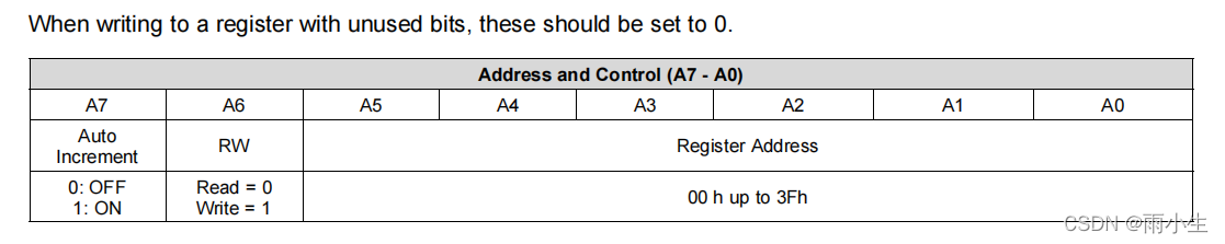
下面介绍一下指令的组成
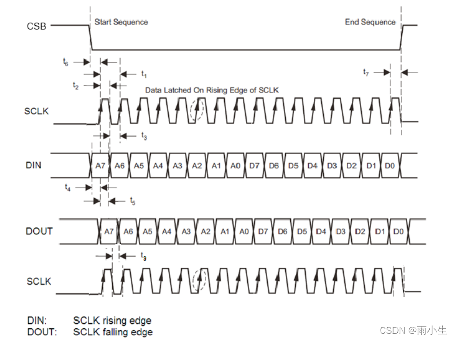
讯享网
还是回到这幅图,从这幅图中看出数据发送为先地址在数据,上升沿TDC读入,下降沿TDC写出。所以我们的指令格式都得遵循地址在前,数据在后的格式。确定数据格式之后,我们根据数据手册中寄存器的地址确定6位地址信息,外加最高位自动增长位和次高位读写位组成8位地址+8位数据的格式,作为一帧数据发送(如下图所示)。
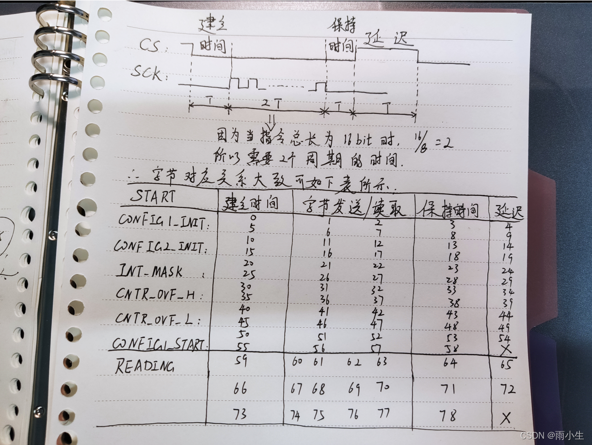
- SPI时钟确定
讯享网always @(posedge sys_clk or negedge sys_rst_n)begin if(!sys_rst_n) sck_cnt <= 2'd0; else if( (state == CONFIG1_INIT && (cnt_byte == 8'd1 || cnt_byte == 8'd2)) || (state == CONFIG1_IN_RD && (cnt_byte == 8'd6 || cnt_byte == 8'd7)) || (state == CONFIG2_INIT && (cnt_byte == 8'd11 || cnt_byte == 8'd12)) || (state == CONFIG2_IN_RD && (cnt_byte == 8'd16 || cnt_byte == 8'd17)) || (state == INT_MASK_INIT && (cnt_byte == 8'd21 || cnt_byte == 8'd22)) || (state == INT_MASK_IN_RD && (cnt_byte == 8'd26 || cnt_byte == 8'd27)) || (state == CNTR_OVF_H && (cnt_byte == 8'd31 || cnt_byte == 8'd32)) || (state == CNTR_OVF_H_RD && (cnt_byte == 8'd36 || cnt_byte == 8'd37)) || (state == CNTR_OVF_L && (cnt_byte == 8'd41 || cnt_byte == 8'd42)) || (state == CNTR_OVF_L_RD && (cnt_byte == 8'd46 || cnt_byte == 8'd47)) || (state == CONFIG1_START && (cnt_byte == 8'd51 || cnt_byte == 8'd52)) || (state == CONFIG1_STA_RD && (cnt_byte == 8'd56 || cnt_byte == 8'd57)) || (state == READING_TDC && (cnt_byte == 8'd60 || cnt_byte == 8'd61 || cnt_byte == 8'd62 || cnt_byte == 8'd63 || cnt_byte == 8'd67 || cnt_byte == 8'd68 || cnt_byte == 8'd69 || cnt_byte == 8'd70 || cnt_byte == 8'd74 || cnt_byte == 8'd75 || cnt_byte == 8'd76 || cnt_byte == 8'd77)) ) sck_cnt <= sck_cnt + 1'd1; else sck_cnt <= sck_cnt; end always @(posedge sys_clk or negedge sys_rst_n)begin if(!sys_rst_n) sck <= 1'b0; else if(sck_cnt == 2'd2) sck <= 1'b1; else if(sck_cnt == 2'd0) sck <= 1'b0; else sck <= sck; end
- 字节数确定
always @(posedge sys_clk or negedge sys_rst_n)begin if(!sys_rst_n) clk_cnt <= 5'd0; else if(state == INITIAL_IDLE || state == ENABLE_LOW || state == ENABLE_HIGH || state == WAITING_TDC || state == WAITING_RESET) clk_cnt <= 5'd0; else if(clk_cnt == 5'd31) clk_cnt <= 5'd0; else clk_cnt <= clk_cnt + 1'd1; end always @(posedge sys_clk or negedge sys_rst_n)begin if(!sys_rst_n) cnt_byte <= 8'd0; else if(cnt_byte == 8'd78 && clk_cnt == 5'd31) cnt_byte <= 8'd78; else if(clk_cnt == 5'd31) cnt_byte <= cnt_byte + 1'd1; else cnt_byte <= cnt_byte; end 正如上面所说的那样,最长的时间就是数据发送的过程,因为TDC的寄存器要么是8位要么是24位。如果我们使用16位作为一个位单元将会十分不方便,所以我们采用每8位作为一个位单元。所以50MHz的主频时钟,12.5MHz的SCK时钟,50 / 12.5 * 8 = 32个单元。至于这边为什么使用全都用32作为一个时钟计数周期,参考火哥的SPI代码时序控制,因为整个时序中最长的时间就是数据发送的过程,那么我们每次都使用这个时间段作时序延时(比如说上一篇文章说到的建立时间、保持时间、CS拉高时间等),这样一来就大大方便了我们编写时序以及省去了大篇幅的代码。

cnt_byte与每个状态对应的时序图以及计数关系表如下所示:
- 两段式状态机状态跳转
根据上图我们编写状态跳转代码如下
讯享网always @(posedge sys_clk or negedge sys_rst_n)begin if(!sys_rst_n) begin state <= INITIAL_IDLE; tdc_en <= 1'b0; end else begin case(state) INITIAL_IDLE:begin state <= ENABLE_LOW; end ENABLE_LOW:begin tdc_en <= 1'b0; if(delay_cnt1 == DELAY_ONE_PART)//50_000_000 state <= ENABLE_HIGH; else state <= ENABLE_LOW; end ENABLE_HIGH:begin tdc_en <= 1'b1; if(delay_cnt2 == DELAY_TWO_PART)//250_000 state <= CONFIG1_INIT; else state <= ENABLE_HIGH; end CONFIG1_INIT:begin if(cnt_byte == 8'd3 && clk_cnt == 5'd31) state <= DELY; else state <= CONFIG1_INIT; end DELY:begin if(cnt_byte == 8'd4 && clk_cnt == 5'd31) state <= CONFIG1_IN_RD; else if(cnt_byte == 8'd9 && clk_cnt == 5'd31) state <= CONFIG2_INIT; else if(cnt_byte == 8'd14 && clk_cnt == 5'd31) state <= CONFIG2_IN_RD; else if(cnt_byte == 8'd19 && clk_cnt == 5'd31) state <= INT_MASK_INIT;//INT_MASK_INIT else if(cnt_byte == 8'd24 && clk_cnt == 5'd31) state <= INT_MASK_IN_RD; else if(cnt_byte == 8'd29 && clk_cnt == 5'd31) state <= CNTR_OVF_H; else if(cnt_byte == 8'd34 && clk_cnt == 5'd31) state <= CNTR_OVF_H_RD; else if(cnt_byte == 8'd39 && clk_cnt == 5'd31) state <= CNTR_OVF_L;//WAITING_TDC else if(cnt_byte == 8'd44 && clk_cnt == 5'd31) state <= CNTR_OVF_L_RD; else if(cnt_byte == 8'd49 && clk_cnt == 5'd31) state <= CONFIG1_START; else if(cnt_byte == 8'd54 && clk_cnt == 5'd31) state <= CONFIG1_STA_RD; else if(cnt_byte == 8'd65 && clk_cnt == 5'd31) state <= READING_TDC; else if(cnt_byte == 8'd72 && clk_cnt == 5'd31) state <= READING_TDC; else state <= DELY; end CONFIG1_IN_RD:begin if(cnt_byte == 8'd8 && clk_cnt == 5'd31) state <= DELY; else state <= CONFIG1_IN_RD; end CONFIG2_INIT:begin if(cnt_byte == 8'd13 && clk_cnt == 5'd31) state <= DELY; else state <= CONFIG2_INIT; end CONFIG2_IN_RD:begin if(cnt_byte == 8'd18 && clk_cnt == 5'd31) state <= DELY; else state <= CONFIG2_IN_RD; end INT_MASK_INIT:begin if(cnt_byte == 8'd23 && clk_cnt == 5'd31) state <= DELY; else state <= INT_MASK_INIT; end INT_MASK_IN_RD:begin if(cnt_byte == 8'd28 && clk_cnt == 5'd31) state <= DELY; else state <= INT_MASK_IN_RD; end CNTR_OVF_H:begin if(cnt_byte == 8'd33 && clk_cnt == 5'd31) state <= DELY; else state <= CNTR_OVF_H; end CNTR_OVF_H_RD:begin if(cnt_byte == 8'd38 && clk_cnt == 5'd31) state <= DELY; else state <= CNTR_OVF_H_RD; end CNTR_OVF_L:begin if(cnt_byte == 8'd43 && clk_cnt == 5'd31) state <= DELY; else state <= CNTR_OVF_L; end CNTR_OVF_L_RD:begin if(cnt_byte == 8'd48 && clk_cnt == 5'd31) state <= DELY; else state <= CNTR_OVF_L_RD; end CONFIG1_START:begin if(cnt_byte == 8'd53 && clk_cnt == 5'd31) state <= DELY; else state <= CONFIG1_START; end CONFIG1_STA_RD:begin if(cnt_byte == 8'd58 && clk_cnt == 5'd31) state <= WAITING_TDC; else state <= CONFIG1_STA_RD; end WAITING_TDC:begin if(tdc_interrupt_flag) state <= READING_TDC; else state <= WAITING_TDC; end READING_TDC:begin if(cnt_byte == 8'd78 && clk_cnt == 5'd31) state <= WAITING_RESET; else if((cnt_byte == 8'd64 || cnt_byte == 8'd71) && clk_cnt == 5'd31) state <= DELY; else state <= READING_TDC; end WAITING_RESET:begin state <= WAITING_RESET; end endcase end end
初始化各个状态和DELY状态之间的跳转便不再多说了,我们看到WAITING_TDC状态下,若收到TDC测时完成的信号,便跳转到读TDC的状态READING_TDC,在这个状态下根据上一篇文章所述,我们需要读取三个寄存器TIME1、CALI1、CALI2所以有三个读取时序,这三个寄存器都是24位的,所以我们在将地址发送过去之后会有三个数据帧的读取(和之前每帧数据2个周期不同,这里会有4个周期),读取完三个寄存器数据之后计算即可得出时间间隔。
- 数据发送
always @(posedge sys_clk or negedge sys_rst_n)begin if(!sys_rst_n) bit_cnt <= 4'd0; //because it is mode 0 else case(cnt_byte) 8'd1,8'd2,8'd6,8'd7,8'd11,8'd12,8'd16,8'd17,8'd21,8'd22,8'd26,8'd27, 8'd31,8'd32,8'd36,8'd37,8'd41,8'd42,8'd46,8'd47,8'd51,8'd52,8'd56,8'd57, 8'd60,8'd61,8'd62,8'd63,8'd67,8'd68,8'd69,8'd70,8'd74,8'd75,8'd76,8'd77:begin if(sck_cnt == 2'd3) //data updata bit_cnt <= bit_cnt + 1'd1; else bit_cnt <= bit_cnt; end default:bit_cnt <= 4'd0; endcase end always @(posedge sys_clk or negedge sys_rst_n)begin if(!sys_rst_n) mosi <= 1'b0; else begin case(cnt_byte) 8'd1, 8'd2: mosi <= CONFIG1_COMMAND[4'd15 - bit_cnt]; 8'd6, 8'd7: mosi <= CONFIG1_READING[4'd15 - bit_cnt]; 8'd11, 8'd12: mosi <= CONFIG2_COMMAND[4'd15 - bit_cnt]; 8'd16, 8'd17: mosi <= CONFIG2_READING[4'd15 - bit_cnt]; 8'd21, 8'd22: mosi <= INTMASK_COMMAND[4'd15 - bit_cnt]; 8'd26, 8'd27: mosi <= INTMASK_READING[4'd15 - bit_cnt]; 8'd31, 8'd32: mosi <= CNTRO_H_COMMAND[4'd15 - bit_cnt]; 8'd36, 8'd37: mosi <= CNTRO_H_READING[4'd15 - bit_cnt]; 8'd41, 8'd42: mosi <= CNTRO_L_COMMAND[4'd15 - bit_cnt]; 8'd46, 8'd47: mosi <= CNTRO_L_READING[4'd15 - bit_cnt]; 8'd51, 8'd52: mosi <= CONFIG1_TO_STAR[4'd15 - bit_cnt]; 8'd56, 8'd57: mosi <= CONFIG1_READING[4'd15 - bit_cnt]; 8'd60, 8'd61: mosi <= READING_TIME1[4'd15 - bit_cnt]; 8'd62, 8'd63: mosi <= READING_SUPP[4'd15 - bit_cnt]; 8'd67, 8'd68: mosi <= READING_CALI1[4'd15 - bit_cnt]; 8'd69, 8'd70: mosi <= READING_SUPP[4'd15 - bit_cnt]; 8'd74, 8'd75: mosi <= READING_CALI2[4'd15 - bit_cnt]; 8'd76, 8'd77: mosi <= READING_SUPP[4'd15 - bit_cnt]; default: mosi <= 1'b0; endcase end end 如上述代码所示,我们根据当前周期可以得到需要发送的数据,再根据高位在前的原则把数据发送出去即可。
- 数据接收与传出
讯享网always @(posedge sys_clk or negedge sys_rst_n)begin if(!sys_rst_n) miso_flag <= 1'b0; else if(sck_cnt == 2'd1 && (cnt_byte == 8'd7 || cnt_byte == 8'd17 || cnt_byte == 8'd27 || cnt_byte == 8'd37 || cnt_byte == 8'd47 || cnt_byte == 8'd57 || cnt_byte == 8'd61 || cnt_byte == 8'd62 || cnt_byte == 8'd63 || cnt_byte == 8'd68 || cnt_byte == 8'd69 || cnt_byte == 8'd70 || cnt_byte == 8'd75 || cnt_byte == 8'd76 || cnt_byte == 8'd77)) miso_flag <= 1'b1; else miso_flag <= 1'b0; end always @(posedge sys_clk or negedge sys_rst_n)begin if(!sys_rst_n) data <= 8'd1; else if(miso_flag == 1'b1) data <= {
   data[6:0],miso}; end always @(posedge sys_clk or negedge sys_rst_n)begin if(!sys_rst_n) data_ok_flag <= 1'b0; else if((cnt_byte == 8'd7 || cnt_byte == 8'd17 || cnt_byte == 8'd27 || cnt_byte == 8'd37 || cnt_byte == 8'd47 || cnt_byte == 8'd57 || cnt_byte == 8'd61 || cnt_byte == 8'd63 || cnt_byte == 8'd68 || cnt_byte == 8'd70 || cnt_byte == 8'd75 || cnt_byte == 8'd77) && (bit_cnt == 4'd15) && (miso_flag == 1'b1)) data_ok_flag <= 1'b1; else if((cnt_byte == 8'd62 || cnt_byte == 8'd69 || cnt_byte == 8'd76) && bit_cnt == 4'd7 && miso_flag == 1'b1) data_ok_flag <= 1'b1; else data_ok_flag <= 1'b0; end always @(posedge sys_clk or negedge sys_rst_n)begin if(!sys_rst_n) data_out_flag <= 1'b0; else data_out_flag <= data_ok_flag; end assign data_out = data_ok_flag ? data : data_out;
因为在SCK下降沿数据被读出,跟警察前面SCK控制时序,当SCK_CNT为0时SCK被拉低,所以我们滞后一个时钟周期将数据读出,也就是通过位拼接实现移位,从而将数据读出,当8位也就是1帧数据被读出之后我们即可得到一次数据,将其传出。
- 脉冲模拟
将程序下载到板子上之前先用modelsim仿真一下,我们在初始化完成之后产生START和STOP脉冲信号,测试FPGA控制TDC的时序,编写脉冲程序以及test bench如下:
module pulse_sim( input wire sys_clk, input wire sys_rst_n, input wire [7:0] data_in, output reg start, output reg stop, output reg interrupt ); reg start_flag; reg [25:0] delay1_reg; reg interrupt_reg; always @(posedge sys_clk or negedge sys_rst_n)begin if(!sys_rst_n) start_flag <= 1'b0; else if(data_in == 8'h81) start_flag <= 1'b1; else start_flag <= start_flag; end always @(posedge sys_clk or negedge sys_rst_n)begin if(!sys_rst_n) delay1_reg <= 26'd0; else if(delay1_reg == 26'd70) //50_000_020 delay1_reg <= delay1_reg; else if(start_flag) delay1_reg <= delay1_reg + 1'd1; else delay1_reg <= 26'd0; end always @(posedge sys_clk or negedge sys_rst_n)begin if(!sys_rst_n)begin start <= 1'b0; stop <= 1'b0; end else begin if(delay1_reg == 26'd50) //50_000_000 start <= 1'b1; else if(delay1_reg == 26'd62) //50_000_012 stop <= 1'b1; else begin start <= start; stop <= stop; end end end always @(posedge sys_clk or negedge sys_rst_n)begin if(!sys_rst_n) interrupt_reg <= 1'b1; else if(stop) interrupt_reg <= 1'b0; else interrupt_reg <= interrupt_reg; end always @(posedge sys_clk or negedge sys_rst_n)begin if(!sys_rst_n) interrupt <= 1'b1; else interrupt <= interrupt_reg; end endmodule 讯享网`timescale 1ns/1ns module tb_tdc_ctrl(); reg sys_clk; reg sys_rst_n; reg miso; always @(posedge sys_clk or negedge sys_rst_n)begin if(!sys_rst_n) miso <= 1'b0; else miso <= !miso; end initial begin sys_clk = 1'b1; sys_rst_n <= 1'b0; #20 sys_rst_n <= 1'b1; end always #10 sys_clk = !sys_clk; wire start; wire stop; wire mosi; wire cs; wire sck; wire tdc_en; wire [15:0] state = u_tdc_hy.u_tdc_ctrl.state; wire [7:0] cnt_byte = u_tdc_hy.u_tdc_ctrl.cnt_byte; wire [1:0] sck_cnt = u_tdc_hy.u_tdc_ctrl.sck_cnt; wire miso_flag = u_tdc_hy.u_tdc_ctrl.miso_flag; wire data_ok_flag = u_tdc_hy.u_tdc_ctrl.data_ok_flag; wire [3:0] bit_cnt = u_tdc_hy.u_tdc_ctrl.bit_cnt; wire [7:0] data = u_tdc_hy.u_tdc_ctrl.data; tdc_hy u_tdc_hy( .sys_clk (sys_clk), .sys_rst_n (sys_rst_n), .miso (miso), .mosi (mosi), .cs (cs), .sck (sck), .tdc_en (tdc_en), .start (start), .stop (stop) ); endmodule
仿真现象
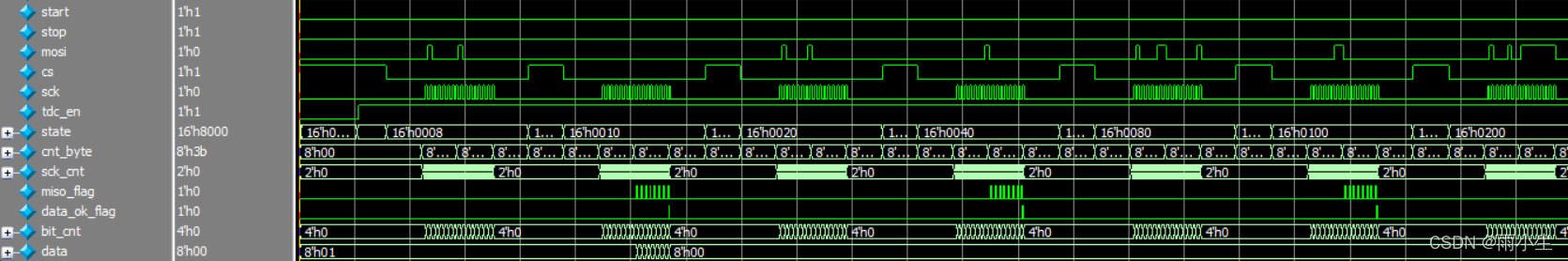
从使能信号被拉下之后的初始化,CS信号、SCK信号以及MOSI都正常。
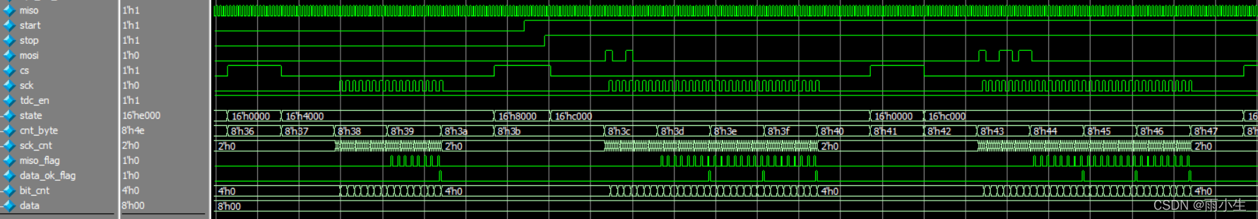
START和STOP信号产生之后我们模拟了一个INTURRUPT信号,之后就是三个24bit的读取,仿真通过,接下来我们上板子来测试一下。
实际测试
由于屏幕显示较为复杂,暂时先不写了,就先用SignalTap来显示一下结果。然后由于身边暂时没有时间间隔产生仪器,所以就先用FPGA自身产生脉冲来作为被测脉冲了。START和STOP间隔设为240ns(12个时钟周期)。
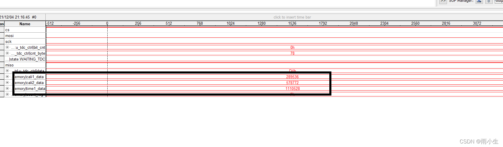
如上图所示为读到的数据,根据上篇文章提到的公式计算:
calCount = (cali2_data - cali1_data) / (2 - 1);
normLSB = CLOCKperiod / calCount;
TOP = TIME * normLSB;
所以有calCount = 289,236,normLSB = (1 / 16M) / 289,236, TOP = * normLSB = 0.23997us = 239.97ns。
误差:abs(239.97 - 240.00) / 240 = 0.125‰;
更换时间间隔为200ns,再次测得数据如下所示:
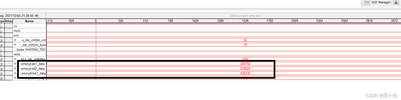
同样的计算方法:
calCount = (cali2_data - cali1_data) / (2 - 1);
normLSB = CLOCKperiod / calCount;
TOP = TIME * normLSB;
有calCount = 289,237,normLSB = (1 / 16M) / 289,237, TOP = * normLSB = 0.20025us = 200.25ns。
误差:abs(200.25 -200.00) / 200 = 1.25‰;
误差分析
(1)逻辑门时间可能会有延迟;
(2)TDC晶振本身精度有限;
(3)没有差分输入+杜邦线传输时钟脉冲导致信号走时不等。
写在最后
附上本文工程代码,本文采用Altera的CYCLONE4系列EP4CE22作为控制器,编译环境为Quartus II 13.1。
链接:https://pan.baidu.com/s/1VQ-v_mxFfIkhN9Qj9XtEBQ
提取码:dpwe
版权声明:本文内容由互联网用户自发贡献,该文观点仅代表作者本人。本站仅提供信息存储空间服务,不拥有所有权,不承担相关法律责任。如发现本站有涉嫌侵权/违法违规的内容,请联系我们,一经查实,本站将立刻删除。
如需转载请保留出处:https://51itzy.com/kjqy/25116.html