
1、器件结构
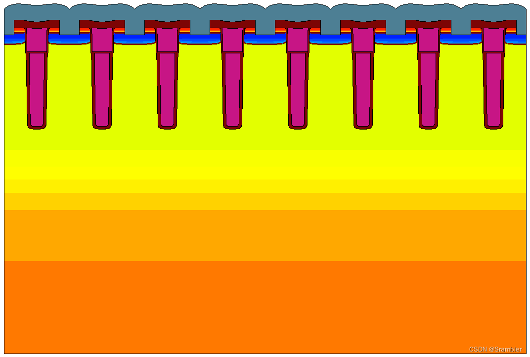
分离栅VDMOS是在传统沟槽栅VDMOS的基础上将栅极分为两段,底部的栅极和源极接相同电位,从而屏蔽了部分栅漏间的电容。该结构有助于减小Miller电容,提高器件的开关速度。
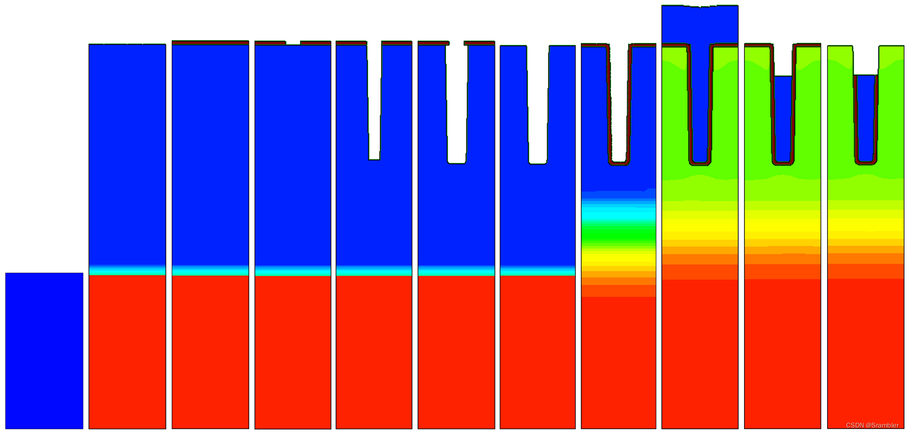
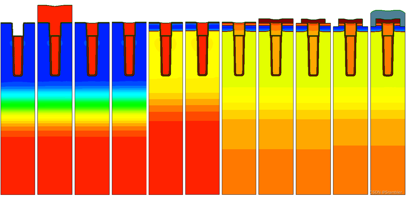
2、工艺流程
分离栅VDMOS的简要工艺流程如下图所示,实际工艺中将包含更多细节:
1) 衬底---> 2) 外延---> 3) 表面氧化---> 4) 光刻氧化层定位沟槽---> 5) 硅刻蚀---> 6) 进一步硅刻蚀---> 7) 去除氧化物---> 8) 沟槽氧化---> 9) 多晶硅淀积---> 10) 多晶硅刻蚀---> 11) 氧化物刻蚀---> 12) 栅氧生长---> 13) 多晶硅淀积---> 14) 多晶硅刻蚀---> 15) P掺杂注入---> 16) 退火激活---> 17) N掺杂注入---> 18) 退火激活---> 19) 氧化物淀积---> 20) 光刻氧化层定位源接触---> 21) 硅刻蚀---> 22) 源极金属淀积

Sentaurus sprocess 工艺仿真代码如下:
------------------------------------------------------------------------ Split-Gate VDMOS Device Process Simulation ------------------------------------------------------------------------ mgoals accuracy= 1e-5 math coord.ucs pdbSet Grid SnMesh min.normal.size 0.005 pdbSet Grid SnMesh normal.growth.ratio.2d 1.5 pdbSet Grid SnMesh max.lateral.size 1.0 refinebox interface.materials= Silicon pdbSet Grid Adaptive 1 pdbSet Grid Min.Adaptive.Temp 1200.0 refinebox name= Global adaptive Silicon \ refine.min.edge= "0.01 0.01" refine.max.edge= "1.0 1.0" \ abs.error= "Boron=1e15 Arsenic=5e16 Phosphorus=1e15" \ rel.error= "Boron=0.20 Arsenic=0.20 Phosphorus=0.20" \ max.dose.error= "Boron=1e10 Arsenic=1e10 Phosphorus=1e10" pdbSet Oxide Grid perp.add.dist 5.0e-7 pdbSet Silicon Grid Remove.Dist 2.0e-8 pdbSet Grid NativeLayerThickness 1.0e-7 pdbSet Diffuse dThickness 6.0e-3 AdvancedCalibration mask name= m_trench segments= {0.8 1.2} negative mask name= m_contact segments= {0.0 0.3 1.7 2.0} negative ------------------------------------------------------------- line x location= 0.0<um> spacing= 0.2<um> tag= top line x location= 1.0<um> spacing= 0.2<um> line x location= 4.0<um> spacing= 0.5<um> tag= bottom line y location= 0.0<um> spacing= 0.2<um> tag= left line y location= 2.0<um> spacing= 0.2<um> tag= right region Silicon xlo= top xhi= bottom ylo= left yhi= right substrate init Silicon field=Phosphorus concentration= 1e19 wafer.orient=100 !DelayFullD struct tdr=1_init refinebox name= ref_int min.normal.size= 0.1 normal.growth.ratio= 5.0 \ interface.materials = { Silicon } min= { -1.0 0.0 } max= { 1.0 2.0 } Epitaxy N-drift layer temp_ramp name= ramp_drift temperature= 550 t.final= 700 time=1<min> temp_ramp name= ramp_drift t.final= 700 time= 5<min> Epi thick= 6<um> \ epi.doping = { phosphorus= 2e16 } diffuse temp.ramp= ramp_drift struct tdr=2_epi Oxide deposition of 100 nm thick deposit oxide thickness= 0.1 isotropic struct tdr=3_oxide trench etching etch oxide thickness=0.11 anisotropic mask= m_trench struct tdr=4_etch Directional etching of Silicon to produce angled trenches etch time= 3 type= trapezoidal material= Silicon rate= 1.0 angle=89 struct tdr=5_etch etch time= 1 type= isotropic material= Silicon rate= 0.1 struct tdr=6_etch strip oxide grid remesh struct tdr=7_etch -- Gate Oxidation temp_ramp name= GateOx time= 80 temperature= 700 t.final= 1100 temp_ramp name= GateOx time= 10 temperature= 1100 t.final= 1100 temp_ramp name= GateOx time= 40 temperature= 1100 t.final= 1100 pressure= 1 flowO2= 12 temp_ramp name= GateOx time= 10 temperature= 1100 t.final= 1100 temp_ramp name= GateOx time= 120 temperature= 1100 t.final= 700 diffuse temp_ramp= GateOx struct tdr=8_oxide Polysilicon Deposition deposit polysilicon type=isotropic thickness=1.0 \ temperature=580 species= Phosphorus concentration= 1.0e19 struct tdr=9_poly etch polysilicon type= cmp coord= -5.2 struct tdr=10_etch etch oxide type= cmp coord= -5.2 struct tdr=11_etch -- Gate Oxidation temp_ramp name= GateOx1 time= 80 temperature= 700 t.final= 1100 temp_ramp name= GateOx1 time= 10 temperature= 1100 t.final= 1100 temp_ramp name= GateOx1 time= 15 temperature= 1100 t.final= 1100 pressure= 1 flowO2= 12 temp_ramp name= GateOx1 time= 10 temperature= 1100 t.final= 1100 temp_ramp name= GateOx1 time= 120 temperature= 1100 t.final= 700 diffuse temp_ramp= GateOx1 struct tdr=12_oxide Polysilicon Deposition deposit polysilicon type=isotropic thickness=1.0 \ temperature=580 species= Phosphorus concentration= 1.0e19 struct tdr=13_poly etch time= 10 type= isotropic material= polysilicon rate= 0.1 struct tdr=14_etch Pwell implant Boron dose= 1.0e13 energy= 80 struct tdr=15_imp temp_ramp name= ramp_npwell time= 10.0<min> temp= 700.0<C> t.final= 850.0<C> temp_ramp name= ramp_npwell time= 1.0<min> temp= 850.0<C> t.final= 850.0<C> temp_ramp name= ramp_npwell time= 10.0<min> temp= 850.0<C> t.final= 700.0<C> diffuse temp_ramp= ramp_npwell struct tdr=16_anneal Nplus implant Arsenic dose= 4.0e15 energy= 80 struct tdr=17_imp temp_ramp name= ramp_nplus time= 10.0<min> temp= 700.0<C> t.final= 850.0<C> temp_ramp name= ramp_nplus time= 1.0<min> temp= 850.0<C> t.final= 850.0<C> temp_ramp name= ramp_nplus time= 10.0<min> temp= 850.0<C> t.final= 700.0<C> diffuse temp_ramp= ramp_nplus struct tdr=18_anneal Oxide Deposition deposit oxide type=isotropic thickness=0.2 struct tdr=19_oxide etch oxide thickness=0.3 anisotropic mask= m_contact struct tdr=20_etch etch silicon thickness=0.2 anisotropic struct tdr=21_etch deposit Aluminum type=isotropic thickness=0.5 struct tdr=22_metal Contact definitions contact name= gate region= PolySilicon_2 !replace contact name= source region= PolySilicon_1 !replace contact name= source1 region= Aluminum_1 !replace contact name= drain box Silicon xlo= 3.9 xhi= 4.1 ylo= -0.1 yhi= 2.1 struct smesh= 23_final讯享网
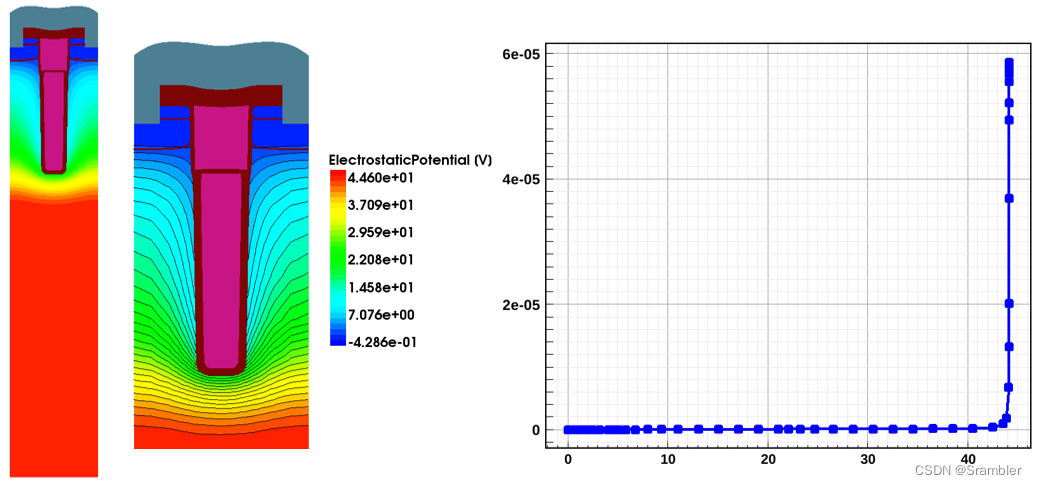
3、 电学特性
该分离栅VDMOS具有44.6V击穿电压,电势分布及击穿特性曲线如下:
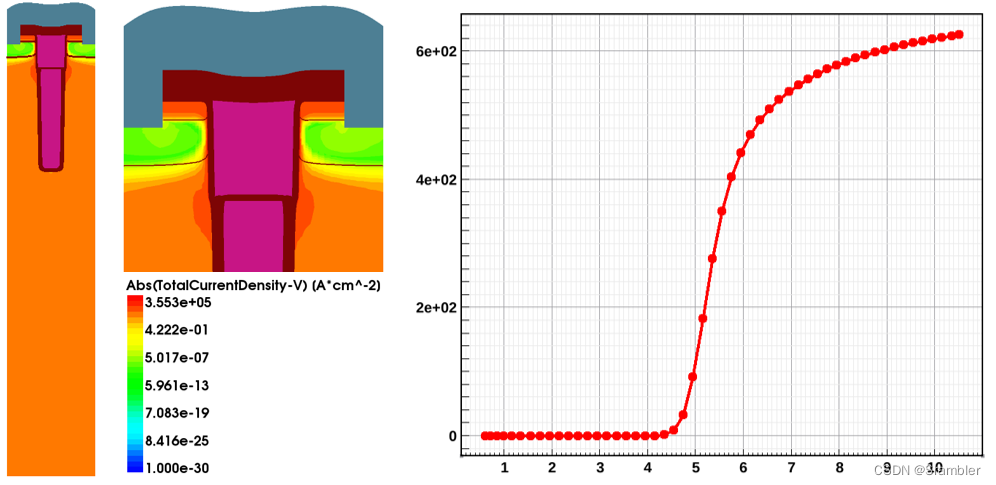
其阈值电压为4.5V,导通电流分布及转移特性曲线如下:
版权声明:本文内容由互联网用户自发贡献,该文观点仅代表作者本人。本站仅提供信息存储空间服务,不拥有所有权,不承担相关法律责任。如发现本站有涉嫌侵权/违法违规的内容,请联系我们,一经查实,本站将立刻删除。
如需转载请保留出处:https://51itzy.com/kjqy/61413.html